 EVERYTHING


An Atomic Wall Halts Microchip Miniaturization
Think of a microchip transistor as a microscopic light switch controlling the flow of digital signals. To turn the switch on and off cleanly, chipmakers place an insulating gate layer directly above the semiconductor channel. For over a decade, physicists have recognized that two-dimensional semiconductors like molybdenum disulfide—sheets of atoms thinner than a strand of DNA—could replace silicon in next-generation processors. However, depositing the necessary insulating layers onto these ultra-thin sheets disrupted their delicate atomic structure, causing moving electrons to scatter and lose momentum.
«For many years, efforts to improve atomically thin transistors largely focused on discovering better semiconductor materials,» explained study corresponding author Professor Wen-Hao Chang. «Our research shows that the atomic interface between materials can be just as important. By engineering that boundary, we were able to reduce one of the fundamental tradeoffs that has limited two-dimensional transistors for many years.»
Engineering a 0.42-Nanometer Buffer Layer
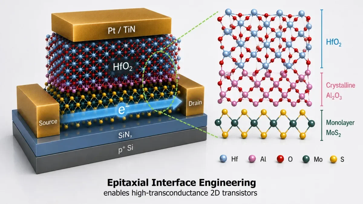
Rather than searching for an entirely new semiconductor, researchers at National Yang Ming Chiao Tung University, collaborating with TSMC Corporate Research, targeted the microscopic junction where the materials connect. The team deposited an ultrathin layer of aluminum directly onto monolayer molybdenum disulfide and carefully oxidized it to form a protective aluminum oxide buffer measuring just 0.42 nanometers in thickness.
According to research published in Nature Electronics on 9 August 2026, this ultra-thin interface performs two simultaneous functions: it creates a uniform template for growing high-dielectric hafnium oxide while acting as an atomic shield that prevents unwanted electrical interference.
In rigorous electrical evaluations, short-channel transistors built with this engineered interface demonstrated outstanding physical metrics:
- Achieved an equivalent oxide thickness of approximately 1 nanometer without degrading electron transport.
- Delivered a peak transconductance of 0.45 mS µm⁻¹ across 100-nanometer channel lengths.
- Maintained low leakage current and minimal hysteresis during high-frequency operational switching.
Moving 2D Electronics From Lab Bench to Wafer Scale
The true significance of this discovery lies in how the material was synthesized. Previous experimental 2D devices relied on microscopic flakes peeled by hand from bulk crystals—a method suitable for laboratory demonstrations but impossible to scale in commercial foundries. By demonstrating this 0.42-nanometer interface on chemical vapor deposition monolayers grown across full semiconductor wafers, the research team proved that 2D transistors can be integrated into industrial production lines.
As microchip components approach atomic dimensions, the physical boundary is no longer simply a passive divider between materials. Instead, it becomes an active, engineered component of the transistor itself, offering semiconductor manufacturers a clear path to continue scaling computer performance beyond the physical boundaries of silicon.