The integration of complex functions into increasingly smaller chips remains a central hurdle in modern semiconductor manufacturing. As devices become more powerful yet physically constrained, traditional methods require adding numerous circuits and transistors, complicating both fabrication and thermal management.
According to Techxplore, researchers at POSTECH (Pohang University of Science and Technology), led by Professor Byoung Hun Lee and Dr. Jae Hyeon Jun, have engineered a solution using zinc oxide (ZnO) and tellurium (Te). This ZnO–Te heterojunction transistor allows for unprecedented functional density in a single component.
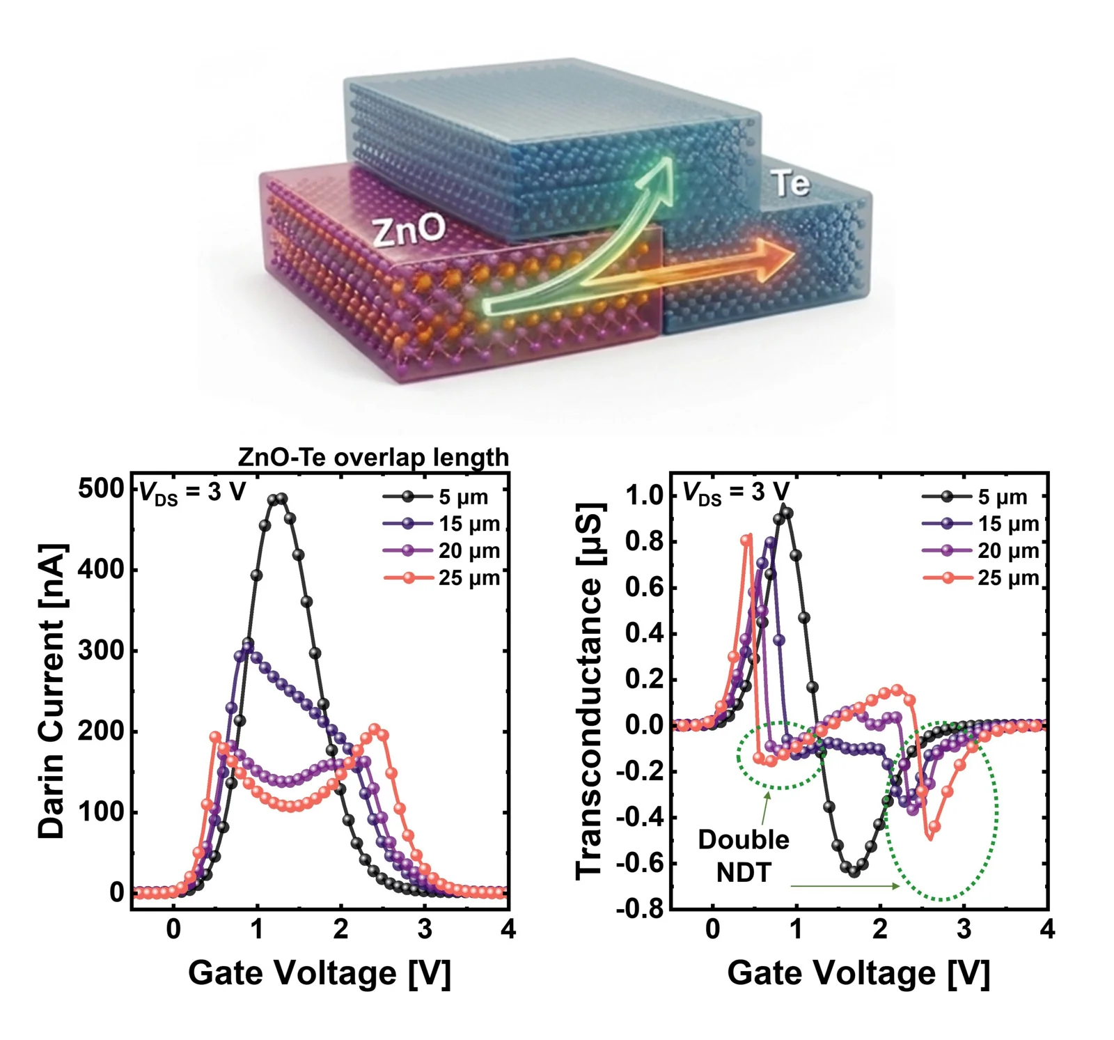
Overcoming Fabrication Limitations
A key constraint in chip design is the temperature required for adding new functions. Back-end-of-line processing must occur below 400 C to protect existing structures. The POSTECH team focused on ZnO and Te because both materials can be fabricated as thin, uniform films at temperatures under 200 C, making them ideal candidates for next-generation, low-heat semiconductor applications.
The device operates distinctively from conventional semiconductors. While standard transistors typically increase current as voltage rises, this new design exhibits negative differential transconductance (NDT), meaning the current decreases over a specific voltage range before changing direction again. The team successfully implemented double NDT (D-NDT), allowing this phenomenon to occur twice in succession within one device.
The Mechanism of Multi-Tasking
In essence, the technology allows one physical component to manage tasks that would normally require several separate devices. This complexity is achieved by precisely controlling the geometric overlap length between the ZnO and Te materials. When the overlap region is short, current changes only once; however, extending this overlap enables both lateral and vertical currents to form simultaneously.
This controlled interaction transforms a simple linear signal path into one capable of complex processing. For instance, using this device, the team implemented a frequency quadrupler—a function that typically demands multiple transistors. The new technology achieves this with just one device, resulting in a 75% reduction in required components. Furthermore, practical circuit experiments confirmed that data processing speed increased fourfold within a single input signal cycle.
Impact on Edge Computing
This breakthrough represents a significant step toward realizing highly efficient edge computing and advanced wearable technologies. By drastically reducing the transistor count while boosting performance, this technology addresses the fundamental conflict between device miniaturization and computational demand. The ability to perform complex functions within a single, low-temperature fabricated component promises to accelerate the deployment of sophisticated AI applications in real-world environments.
The development demonstrates that next-generation semiconductor design can move beyond simple binary switching toward highly integrated, multi-functional processing units.