According to Thequantuminsider, researchers at the University of Illinois have successfully developed a scalable, low-temperature process for monolithic 3D chip integration. This innovation addresses one of the most persistent technical hurdles in advanced semiconductor manufacturing: maintaining high performance while stacking multiple silicon layers vertically.
The Limits of Traditional Scaling
For over half a century, the exponential growth of computing power has been driven primarily by shrinking transistors and packing them more densely onto flat surfaces. However, as devices approach atomic dimensions, they begin to encounter fundamental limitations imposed by quantum effects and physical constraints. The next major leap in computational capability requires moving beyond two-dimensional scaling and embracing vertical integration.
Monolithic 3D integration—the process of building each layer directly on top of the previous one—is considered the most efficient approach for maximizing interlayer connectivity. However, achieving this has historically been fraught with difficulty due to extreme temperature requirements. Standard fabrication processes typically necessitate temperatures around 1,000 degrees Celsius. For upper layers beyond the first, the thermal budget is strictly limited to 400 degrees Celsius; exceeding this limit risks destroying delicate metal wiring and compromising device integrity.
Achieving High Performance Under Thermal Constraints
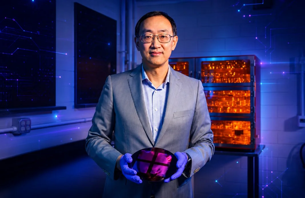
A team led by Associate Professor Qing Cao of Illinois Grainger Engineering has demonstrated a novel solution that successfully operates within this critical temperature constraint. Their newly invented process utilizes single-crystalline silicon, the standard semiconductor material used across the industry, and maintains high device performance across multiple tiers.
The researchers showcased three vertically stacked layers, with each layer containing 625 transistors. Crucially, they achieved impressive device yields ranging from 98% to 100%, even within an academic laboratory cleanroom environment. This high yield rate indicates strong potential for eventual industrial adoption.Associate Professor Cao explained the functional benefit of this vertical approach: “Take something as simple as static random-access memory, which is universal in CPUs and GPUs. Today it takes six microelectronic devices called transistors on a single plane to store one bit of information. With vertical integration, you can distribute them across multiple layers.” He further likened the process to urban planning: “It’s like replacing a sprawling suburb with high-rises: you get the same functionality, but the spatial footprint is reduced while making communication between layers faster and more efficient.”
Implications for Future Computing
While vertical integration is already appearing in specialized AI hardware, monolithic integration represents the key to unlocking the full potential of 3D chips. By stacking circuits, chipmakers can dramatically increase computing density and speed while simultaneously reducing energy consumption per operation. This capability directly supports the ongoing need for more powerful and efficient processors in fields ranging from artificial intelligence training to complex scientific modeling.
The successful demonstration by the University of Illinois provides a robust blueprint for manufacturers seeking to extend Moore’s law into the third dimension, paving the way for next-generation computing architectures that are both denser and more energy-efficient. This breakthrough solidifies 3D integration as a viable, high-yield path forward in modern semiconductor development.